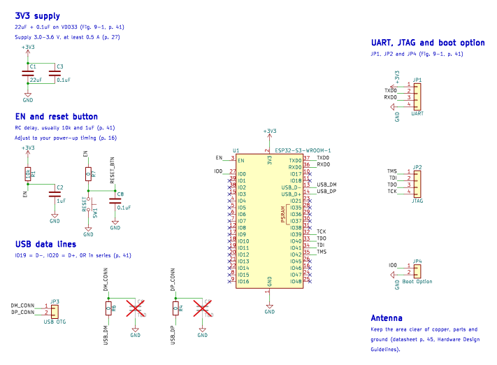
ESP32-S3-WROOM-1 module with the peripheral circuit from Espressif's datasheet: 3V3 decoupling, EN reset network and button, USB D+/D- with series resistors, UART, JTAG and boot-option headers.
DraftMCU module16 partsApache-2.0
Draft. Nobody has checked this against the datasheet yet. It follows ESP32-S3-WROOM-1 & ESP32-S3-WROOM-1U Datasheet v1.8, KiCad opens it without errors, and the nets match the specification. Check the values yourself before you build it.
The schematic as KiCad draws it. Open it at full size to zoom: it is a vector image.
Pins used on ESP32-S3-WROOM-1
Pin numbers follow the datasheet's pin table. Every other pin is marked no-connect (X), so you can see what is free; delete the marker to use a pin.
Pin
Name in KiCad
Net
1
GND
GND
2
3V3
+3V3
3
EN
EN
13
USB_D-
USB_DM
14
USB_D+
USB_DP
27
IO0
IO0
32
IO39
TCK
33
IO40
TDO
34
IO41
TDI
35
IO42
TMS
36
RXD0
RXD0
37
TXD0
TXD0
40
GND
GND
41
GND
GND
Checklist
Required
Supply VDD33 within 3.0 to 3.6 V (3.3 V typical) and able to deliver at least 0.5 A. (Espressif Systems, p. 27, Recommended Operating Conditions)
Fit 22 uF and 0.1 uF on the 3V3 pin as in the reference schematic. (Espressif Systems, p. 41, Figure 9-1)
EN needs the RC delay (usually 10 kOhm and 1 uF) so the supply is stable before the chip starts. Check it against your power-up timing: the rails need at least 50 us to stabilise before EN goes high, and EN must stay low for at least 50 us to reset. (Espressif Systems, p. 41, note under Figure 9-1; timing in Table 4-6, p. 16)
To enter download mode, GPIO0 must be low (and GPIO46 low, its default) while EN is released. GPIO0 has a weak internal pull-up, so with nothing connected the chip boots from flash. (Espressif Systems, p. 14, Tables 4-1 and 4-3)
Strapping pins GPIO0, GPIO3, GPIO45 and GPIO46 are read at reset (hold time at least 3 ms after EN goes high). Do not let connected circuits drive them to a level you did not intend at that moment. (Espressif Systems, p. 14, Table 4-2)
USB uses IO19 (D-) and IO20 (D+), pins 13 and 14. The reference keeps 0 ohm series resistors R6 and R4 on both lines; C5 and C6 are placeholders with no value and not fitted. (Espressif Systems, p. 41, Figure 9-1)
On modules with octal PSRAM (R8 and R16V variants), IO35, IO36 and IO37 are connected to the PSRAM and unavailable. Do not use pins IO35 to IO37 with those variants. (Espressif Systems, p. 12, pin table note b)
The module has an on-board antenna. Keep the antenna area free of copper, ground pour and components, and place the module at the board edge as the Hardware Design Guidelines describe. Check the footprint against the recommended land pattern. (Espressif Systems, p. 45, Figure 11-1 (antenna area); keepout zone note, p. 10)
Recommended
Place C1 and C3 as close to the module's 3V3 pin as practical, with a short return to the ground pad. (common practice)
GPIO45 selects the flash/PSRAM voltage (VDD_SPI) and GPIO3 the JTAG signal source. Leave both at their defaults (weak pull-down and floating) unless you know why you need otherwise. (Espressif Systems, p. 13, Table 4-1)
Soldering the exposed ground pad (EPAD) is optional but improves thermal performance. Use the right amount of solder paste: too much lifts the module and spoils the other joints. (Espressif Systems, p. 41, note under Figure 9-1)
Good to know
UART0 (TXD0 pin 37, RXD0 pin 36) is on JP1 for programming and logs. JTAG (TMS IO42, TDI IO41, TDO IO40, TCK IO39) is on JP2. (Espressif Systems, p. 41, Figure 9-1)
On the R16V variants, IO47 and IO48 work at 1.8 V, not 3.3 V. (Espressif Systems, p. 12, pin table note c; also Figure 9-1)
PCB layout
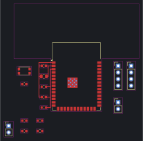
16 footprints, placed around the chip, with 9 tracks for the critical nets (decoupling, ground, reset). The rest is left as a ratsnest: you route it, because the right routing depends on your stack-up and board., drawn for KiCad and checked with its design rule check and schematic comparison. The block has no board outline: it takes the one of the board you place it on.
The layout as KiCad draws it: front copper red, back copper blue.
Keep copper, tracks, vias and other parts out of the antenna zone: the 48 mm wide, 21 mm deep area beyond the module's antenna end, which is part of the footprint's courtyard (KiCad's footprint draws it). Put the antenna end at, or just past, the board edge. (common practice)
Do not place a ground plane or copper under the antenna part of the module on any layer. (common practice)
The 22 uF and 0.1 uF decoupling capacitors sit at the module's 3V3 pin, on the side away from the antenna. (common practice)
Partly routed: the 3V3 decoupling capacitors, the module's ground pin and the EN reset network (pull-up resistor, capacitor, series resistor) are routed on the front layer. The rest is positioned and left as a ratsnest. Route it yourself, with ground pour under and around the module body except at the antenna. (common practice)
Parts list
Ref
Value
KiCad symbol
Footprint
Source
U1
ESP32-S3-WROOM-1
RF_Module:ESP32-S3-WROOM-1
RF_Module:ESP32-S3-WROOM-1
Espressif Systems, p. 41, Figure 9-1 Peripheral Schematics; pin table pp. 10-11
C1
22uF
Device:C
Capacitor_SMD:C_0805_2012Metric
Espressif Systems, p. 41, Figure 9-1, C1 on VDD33
C3
0.1uF
Device:C
Capacitor_SMD:C_0603_1608Metric
Espressif Systems, p. 41, Figure 9-1, C3 on VDD33
R1
10k
Device:R
Resistor_SMD:R_0603_1608Metric
Espressif Systems, p. 41, Figure 9-1 R1 (value TBD there); note: RC delay at EN, usually R = 10 kOhm
C2
1uF
Device:C
Capacitor_SMD:C_0603_1608Metric
Espressif Systems, p. 41, Figure 9-1 C2 (value TBD there); note: RC delay at EN, usually C = 1 uF
R7
0
Device:R
Resistor_SMD:R_0603_1608Metric
Espressif Systems, p. 41, Figure 9-1, R7 in series with the reset switch
SW1
RESET
Switch:SW_Push
Button_Switch_SMD:SW_Push_1P1T_NO_CK_KMR2
Espressif Systems, p. 41, Figure 9-1, SW1
C8
0.1uF
Device:C
Capacitor_SMD:C_0603_1608Metric
Espressif Systems, p. 41, Figure 9-1, C8 across the reset switch
Espressif Systems, p. 41, Figure 9-1, JP4 Boot Option (IO0 to GND)
How to use it
In KiCad 9 or later. Unzip the download. Open Preferences › Manage Design Block Libraries, add the unzipped crossprobe.kicad_blocks folder as a library, then place the block from the design block chooser. The symbols and footprints are KiCad's own.
In Crossprobe. Choose Open in Crossprobe above. It opens a new project with this block already in its schematic, using the reference designators from the table above. The project stays in your browser until you save it, and you pick where it goes. To add the block to a project you already have, open that project, turn on Edit and use Add block.
Source
ESP32-S3-WROOM-1 & ESP32-S3-WROOM-1U Datasheet v1.8, Espressif Systems. Page numbers on this page refer to that version of the document. Values and pin assignments are quoted as facts, with page numbers; the circuit is drawn here, not copied.