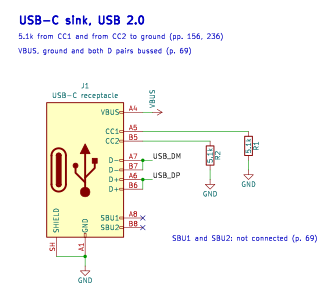
A USB-C receptacle for a device that takes 5 V from a USB-C source and uses USB 2.0 data: the two 5.1 kΩ pull-downs on CC1 and CC2, the VBUS, ground and data pins bussed as the Type-C specification requires, and the unused SBU pins left open.
DraftConnector3 partsApache-2.0
Draft. Nobody has checked this against the datasheet yet. It follows USB Type-C Cable and Connector Specification, Release 2.0 (August 2019), KiCad opens it without errors, and the nets match the specification. Check the values yourself before you build it.
The schematic as KiCad draws it. Open it at full size to zoom: it is a vector image.
Pins used on USB-C receptacle
Pin numbers follow the datasheet's pin table. Every other pin is marked no-connect (X), so you can see what is free; delete the marker to use a pin.
Pin
Name in KiCad
Net
A1
GND
GND
A4
VBUS
VBUS
A5
CC1
Net-(J1-CC1)
A6
D+
USB_DP
A7
D-
USB_DM
A9
VBUS
VBUS
A12
GND
GND
B1
GND
GND
B4
VBUS
VBUS
B5
CC2
Net-(J1-CC2)
B6
D+
USB_DP
B7
D-
USB_DM
B9
VBUS
VBUS
B12
GND
GND
SH
SHIELD
GND
Checklist
Required
A device that takes power from a USB-C port terminates both CC1 and CC2 to ground with pull-down resistors, called Rd. A source recognises the sink by Rd, and the sink knows a source is attached by power appearing on VBUS. (USB 3.0 Promoter Group, p. 156, Sink functional model, Figure 4-9)
Rd is 5.1 kOhm. A +/-20% resistor works, but with it the sink cannot detect the current the source advertises; a +/-10% resistor can (Table 4-25). Use 1% resistors and you can add current detection later. (USB 3.0 Promoter Group, p. 236, Table 4-25 Sink CC Termination (Rd) Requirements)
Connect all four VBUS pins together and all four ground pins together at the receptacle, on the board. Unused contact locations must be left unconnected. (USB 3.0 Promoter Group, p. 69, Table 3-5, notes 1, 4 and 5)
For USB 2.0 the receptacle has two D+ pins (A6, B6) and two D- pins (A7, B7), because the plug can go in either way. Connect the two D+ pins together and the two D- pins together, as close to the receptacle as possible. The shorting trace should be no longer than 3.5 mm. (USB 3.0 Promoter Group, p. 69, Table 3-5, note 2)
Leave SBU1 and SBU2 not connected unless you need them for a specific purpose, such as audio adapter accessory mode. (USB 3.0 Promoter Group, p. 69, Table 3-5, note 3)
Recommended
Add ESD protection on VBUS and the data lines close to the receptacle, and bulk capacitance on VBUS as your regulator's datasheet asks. Neither is in this block; both are common practice. (common practice)
Good to know
A USB 2.0-only sink that needs only default power, and does not use USB Power Delivery or accessories, may treat VBUS appearing as the connection. You then get default USB power only; the Type-C specification defers the limits to the USB 2.0 specification. (USB 3.0 Promoter Group, p. 171, Sec. 4.5.2.2.3.2; Table 4-17 on p. 217)
This block is a sink with Rd only. It does not negotiate: no USB Power Delivery, no 9 V, 12 V or 20 V, and no 1.5 A or 3 A. For those you need a PD controller on CC, and the choice of Rd tolerance and extra circuitry changes. (USB 3.0 Promoter Group, p. 236, Table 4-25)
PCB layout
3 footprints, 10 tracks and 2 vias, drawn for KiCad and checked with its design rule check and schematic comparison. The block has no board outline: it takes the one of the board you place it on.
The layout as KiCad draws it: front copper red, back copper blue.
Place the receptacle at the board edge, with its shield tabs through the board. The shell is tied to ground through the through-hole shield pads, joined on the back layer. (common practice)
Route D+ and D- together, short, and on one layer where you can. Here the two D+ pads are joined north of the pad row and the two D- pads south of it, so neither pair crosses the other. (common practice)
Keep the two 5.1 k CC resistors close to the receptacle; their ground return runs to the back layer through a via each. (common practice)
The VBUS bar is a 0.4 mm track for the pads' sake only. Size VBUS copper for the current you draw (0.5 A at 5 V for a default USB device, up to 3 A advertised). (common practice)
Parts list
Ref
Value
KiCad symbol
Footprint
Source
J1
USB-C receptacle
Connector:USB_C_Receptacle_USB2.0_16P
Connector_USB:USB_C_Receptacle_HRO_TYPE-C-31-M-12
USB 3.0 Promoter Group, p. 69, Table 3-5, receptacle pin assignments for USB 2.0-only support
R1
5.1k
Device:R
Resistor_SMD:R_0402_1005Metric
USB 3.0 Promoter Group, p. 236, Table 4-25, Rd 5.1 kOhm
R2
5.1k
Device:R
Resistor_SMD:R_0402_1005Metric
USB 3.0 Promoter Group, p. 236, Table 4-25, Rd 5.1 kOhm
How to use it
In KiCad 9 or later. Unzip the download. Open Preferences › Manage Design Block Libraries, add the unzipped crossprobe.kicad_blocks folder as a library, then place the block from the design block chooser. The symbols and footprints are KiCad's own.
In Crossprobe. Choose Open in Crossprobe above. It opens a new project with this block already in its schematic, using the reference designators from the table above. The project stays in your browser until you save it, and you pick where it goes. To add the block to a project you already have, open that project, turn on Edit and use Add block.