Fabrication outputs
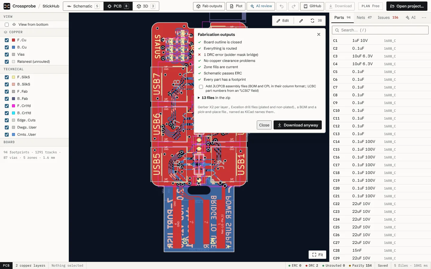
Fab outputs in the top bar checks the board for the usual first-order mistakes, then downloads one zip with Gerbers, drill files, a BOM and a pick-and-place file, named the way KiCad names them.
Export the files
- Open a project with a board and choose Fab outputs in the top bar. The PCB view opens with the Fabrication outputs panel.
- Read the pre-flight list and fix what it flags.
- Optionally tick Add JLCPCB assembly files.
- Expand files in the zip to see the file names.
- Choose Download zip. The zip is named after the board, ending in
-fab.zip.
The files are generated in the browser from the board as it is now, including unsaved edits.
The pre-flight check
Each line is a pass, a warning or a problem:
| Check | When it fails |
|---|---|
| Board outline is closed | Problem. Draw one with the Outline tool, see PCB editing. |
| Everything is routed | Problem. The line counts the unrouted connections. |
| No hole, annular ring or courtyard errors | Problem. The line names the kinds of DRC error. |
| No copper clearance problems | Problem. The line counts shorts and clearance violations. |
| Zone fills are current | Warning, with Refill now. |
| Schematic passes ERC | Warning. The line counts ERC errors. |
| Every part has a footprint | Warning. The line counts parts without one. |
While a problem remains, the button reads Download anyway: the files may not be what you want to order. Warnings don't change the button. Details of each finding are in the Issues tab.
What's in the zip
- Gerber X2, one file per layer: copper, solder mask, paste, silkscreen and the board outline.
- Excellon drill files, plated and non-plated holes separately.
- BOM, a CSV grouped by value, footprint and part number. Its Datasheet column holds each part's datasheet link, plus where its pinned datasheet evidence is.
- Pick-and-place, a CSV position file identical to KiCad's.
Board-only footprints made with Logo or image… are kept out of the BOM and the position file.
Text is drawn in KiCad's own stroke font and laid out as KiCad lays it out. TrueType text uses the glyph outlines KiCad caches in the board file.
JLCPCB assembly files
Add JLCPCB assembly files adds a BOM and a CPL in JLCPCB's column format. LCSC part numbers come from a field named LCSC on each part, which you can add in the schematic with + Add field. The setting is remembered in this browser.
How close to KiCad's plots
Against KiCad's own plots of its demo boards, every layer, silkscreen text included, covers the same shapes within 1%, most of them exactly. The holes are the same, and the position files are identical.
Note: before ordering, check the fab's current limits. Board setup has presets with JLCPCB's published 2- and 4-layer capabilities.