Navigate and cross-probe
One selection drives every view. Pick a part or a net in the schematic, on the board, in 3D or in the inspector, and the others follow it, opening the right sheet when they need to.
The three views
The top bar switches between Schematic (S), PCB (B) and 3D (3). F or the Fit button frames the sheet or the board.
The left panel changes with the view:
- Schematic: the Sheets tree of the hierarchy. Click a sheet to open it. The breadcrumb above the drawing shows the sheet's path and file. In view mode, double-clicking a sheet symbol opens that sheet.
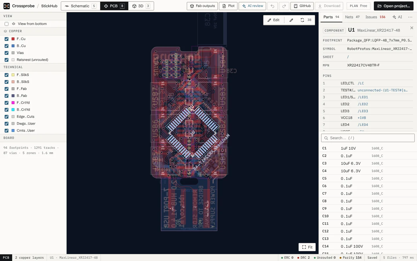
- PCB: layer visibility and board statistics (footprints, tracks, vias, zones, thickness).
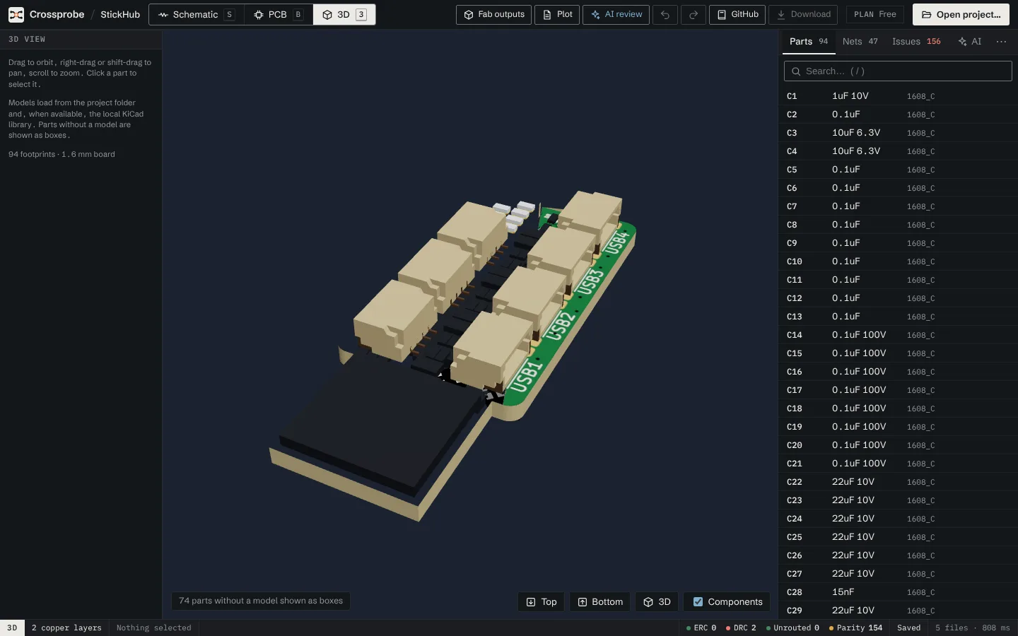
- 3D: how to move around, and the board's footprint count and thickness.
The status bar at the bottom shows the view, what is selected and the check results. Click the check results to open the Issues tab.
Select and cross-probe
Click a part to select it, or a wire, label or pin to select its net. On the board, a part's body selects the part and copper selects its net. A pad selects that pad, and the inspector shows its net, pin, shape, size, drill and layers.
The selection is shared. A part or net picked anywhere is highlighted in the schematic and on the board, and the inspector shows its details. If it is on another sheet, that sheet opens. Esc clears the selection.
Right-click on the board for a menu of what's under the cursor, such as Select net or Zoom to fit.
The inspector
The panel on the right has three tabs for the design itself:
- Parts: every component with its reference, value and footprint, tagged when it has no footprint. A selected part shows its footprint, symbol, datasheet link, sheet, other fields and its pins. Each pin's net is a link that selects that net.
- Nets: every net with its node count. A selected net shows the sheets it is on and the pins it connects, each linked to its part.
- Issues: ERC, DRC, unrouted connections and schematic/PCB parity in one list.
The inspector also holds the AI review, Datasheet and Find parts tabs. See AI design review.
Search
/ (or ⌘F) puts the cursor in the inspector's search box. On Parts it matches reference, value and footprint. On Nets it matches the net name and its aliases. Long lists show the first entries; type more to narrow them.
Issues and markers
The Issues tab groups findings by check. All, ERC and Board filter them, and Errors only hides warnings. Board findings include Clearance (DRC), the other DRC checks, Unrouted connections and Board ↔ schematic.
Click a finding to go to it. An ERC finding opens its sheet at a KiCad-style marker, and a DRC finding jumps to its marker on the board. The checks re-run after every edit, so the list stays current while you work.
Some findings come with a fix. On an unconnected pin, No-connect adds a no-connect flag, and No-connect all flags every pin in the group as one undoable edit. Add PWR_FLAG places a PWR_FLAG on an undriven power pin. On a DRC finding, Exclude asks why it is fine and saves the exclusion in the project file, as KiCad does. Excluded findings sit under Excluded (DRC), where Include checks them again.
KiCad difference: KiCad honours an exclusion made in Crossprobe only where Crossprobe's marker position and item order match its own. Elsewhere KiCad asks again. Exclusions made in KiCad apply in Crossprobe.
Layers and the ratsnest
On the PCB view, the left panel lists the Copper layers, Vias, Ratsnest (unrouted) and the Technical layers (silkscreen, fabrication, courtyards, Edge.Cuts, Dwgs.User, Cmts.User). Tick a layer to show or hide it. View from bottom flips the board to show the back side.
Ratsnest lines show the connections that are still missing. They cover pads, tracks, vias, zone fills and copper shapes, and update after every edit. Pads show their number and net, and tracks and vias show their net names once they are large enough to read.
3D
The 3D view extrudes the board outline with its holes and cutouts and textures both sides with mask, copper and silkscreen. Drag to orbit, right-drag or Shift-drag to pan, and scroll to zoom. Click a part to select it.
Models load from the project folder and, when available, the local KiCad library. Parts without a model are shown as boxes. If a model path uses a variable that isn't available in the browser, such as a company's own library variable, the view names it.
Next: start editing in the schematic or on the board. All keys are on Keyboard shortcuts.