PCB editing
Press E or Edit above the board. The editor follows KiCad's mouse and keys where it can, and move, rotate and flip give the same result as in KiCad's pcbnew.
Select
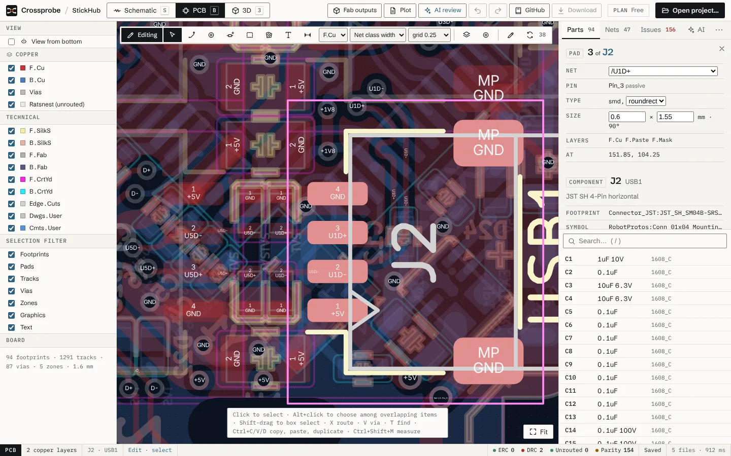
- A pad selects that pad, a part's body the part, and copper its net.
- Alt+click lists everything under the cursor to choose from.
- Shift-drag box-selects. U takes the whole trace.
- Right-click opens a menu for what's under the cursor: rotate, flip, lock, copy, duplicate, delete, select trace or net. On an empty board it offers paste, add footprint, route, measure, refill and fit.
In edit mode the left panel adds a Selection filter with Footprints, Pads, Tracks, Vias, Zones, Graphics and Text. Untick a kind and clicks and boxes no longer pick it.
Move, rotate, flip and lock
Drag to move on the grid. Tracks attached to a moved part stretch along. Arrows nudge.
- R rotates and F flips to the other side.
- L locks. Locked items don't move, rotate, flip or delete; the hint line says so if you try. Press L again to unlock.
- ⌘C, ⌘V and ⌘D copy, paste and duplicate. Copies get fresh UUIDs and the next free reference.
- A part's reference or value can be dragged on its own, as in KiCad.
The grid menu in the toolbar sets the step, from 0.05 to 2.54 mm. N and ⇧N step through it. ⌃⇧M measures between two points, snapping to pads, and shows the distance, dx and dy.
The properties panel
The panel edits what is selected:
- Track: width and layer, with its length. For length tuning, see Routing.
- Via: diameter and drill.
- Footprint: X, Y, rotation and side (Top or Bottom).
- Zone: net, layer and pad connection. See Zones and pours.
- Text: content, size and side.
- Rectangle, such as a rectangular outline: width and height.
A selected pad shows its net, pin, type, shape, size, drill and layers in the inspector. In edit mode you can change its net, shape, size and drill.
Footprints
Footprint (A) places board-only footprints such as mounting holes, fiducials and logos from KiCad's libraries. Search, for example "mountinghole m3", pick one and click to place it. T asks for a reference, then selects that footprint on the board.
Footprints for schematic parts come from the schematic: assign them there, then run Update PCB from schematic.
Logo or image… in the footprint picker traces a PNG, JPEG or SVG into a footprint by a black-and-white threshold, optionally inverted. It goes on the front silkscreen, on copper or as a bare mask opening, and is kept out of the BOM and position files. Placed while you view the board from the bottom, it goes on the back.
Board outline and mounting holes
- Choose Outline. The toolbar's shape menu offers Rectangle, Rounded with a 1, 2 or 3 mm radius, or Polygon.
- For a rectangle, click one corner and then the opposite one. For a polygon, click to add corners and finish by clicking the first corner, double-clicking or pressing Enter. Backspace removes the last corner.
- Select the outline to set its width and height in the properties panel.
To replace an outline, delete it first. Once the board has an outline, 4 × M3 holes places four M3 mounting holes 3.5 mm in from its corners.
Text and dimensions
Text places silkscreen text on F.SilkS, or mirrored on B.SilkS while you view from the bottom. Its content, size and side are in the properties panel.
Dimension: click two points, then move out to set the offset and click to place it on Dwgs.User. O switches between aligned and horizontal/vertical.
KiCad difference: a radial dimension shows only its text.
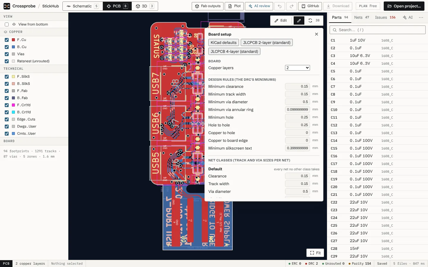
Board setup
Setup opens Board setup, saved in the .kicad_pro as KiCad's Board Setup saves it:
- Presets: KiCad defaults, JLCPCB 2-layer (standard) and JLCPCB 4-layer (standard). The 4-layer preset also sets four copper layers and writes JLCPCB's JLC04161H-7628 stackup. Check the fab's current limits before ordering.
- Copper layers: 2, 4, 6 or 8. Inner layers go between F.Cu and B.Cu, as in KiCad. You can only go down once nothing is left on the layers that would go.
- Design rules: the DRC's minimums for clearance, track width, via diameter and annular ring, hole size, hole to hole, copper to hole, copper to board edge and silkscreen text height.
- Net classes: clearance, track width, via diameter and drill, and pair width and gap per class. Default takes every net no other class takes. Each other class takes nets by name or pattern (
*and?wildcards) and shows how many nets match. + Add net class adds a class, and deleting one sends its nets back to Default.
Each class also shows the current its track width carries at a 10 °C rise. With a stackup, it shows an estimate of the pair's differential impedance, and Size for 90 Ω (USB) sets the pair width for it. For controlled impedance, order it and let the fab size the pair.
Clearance DRC runs after every edit and shows on the board and in the Issues tab. Clearance rules from a custom .kicad_dru file are applied too. See file support.